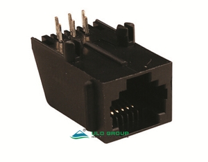

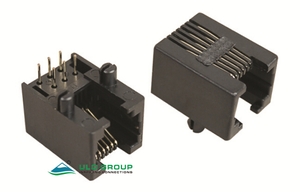
| Part Number: | ULO | - | PJ521 | - | S | 6 | 0 | B | P | S |
|---|---|---|---|---|---|---|---|---|---|---|
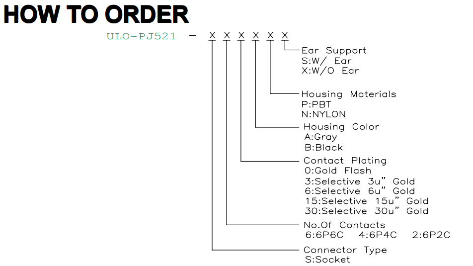
| Explanation: |
Brand ULO - ULO |
Model PJ521 - Six-position socket with material and ear options |
Connector Type S - Socket |
Contacts 2 - 6P2C; PJ521 only |
Plating 0 - Gold flash; all models |
Colour A - Grey; PJ521, PJ521B and PJ521C |
Material Selector P - PBT; PJ521 and PJ521A |
Ear Support S - With ears; PJ521 and PJ521B |
This series contains four unshielded, single-port modular PCB sockets. Six housing positions can contain two, four or six populated contacts depending on the model. P denotes positions and C denotes contacts. Each model uses through-hole termination and has its own mechanical drawing.
| Model | Contact configurations and codes | Insulator | Flammability | Contact resistance |
|---|---|---|---|---|
| ULO-PJ521 | 2: 6P2C; 4: 6P4C; 6: 6P6C | PBT or nylon | UL94V-0 or UL94V-2 | Unspecified |
| ULO-PJ521A | 4: 6P4C; 6: 6P6C | PBT or nylon | UL94V-0 or UL94V-2 | Unspecified |
| ULO-PJ521B | 4: 6P4C; 6: 6P6C | Glass-filled PBT | UL94V-0 | ≤50mΩ |
| ULO-PJ521C | 4: 6P4C; 6: 6P6C | PBT | UL94V-0 | ≤50mΩ |
PJ521 and PJ521A flammability options are not assigned to individual polymers. PJ521B is the vertical socket configuration; follow its drawing for board orientation and mounting clearance.
| Characteristic | Value |
|---|---|
| Insulation resistance | ≥1000MΩ |
| Dielectric withstand test | 500VAC for 1 minute |
| Mating life | ≥600 cycles |
| Contact material | Copper alloy |
| Insulation material group | I |
Working voltage, current rating and operating temperature are unspecified. The dielectric withstand value is a test condition.
| Ordering field | PJ521 | PJ521A | PJ521B | PJ521C |
|---|---|---|---|---|
| Connector type | S: socket | S: socket | S: socket | S: socket |
| Gold flash | 0 | 0 | 0 | 0 |
| 3µin gold | 3: selective | 3: gold; plating area unspecified | 3: selective | 3: selective |
| 6µin, 15µin or 30µin gold | 6 / 15 / 30: selective | 6 / 15 / 30: gold; plating area unspecified | Thickness options; exact suffix unspecified | Thickness options; exact suffix unspecified |
| Housing colour | A: grey; B: black | B: black | A: grey; B: black | A: grey; B: black |
| Material selector | P: PBT; N: nylon | P: PBT; N: nylon | No selector | No selector |
| Support ears | S: with ears; X: without ears | No selector | S: with ears; X: without ears | No selector |
Dimensions are in millimetres. The six-hole drawings show the full contact pattern; the chosen version determines contact population. Mating-contact pitch is 1.02mm on all four models, while PCB tail pitch differs.
| PCB reference | PJ521 | PJ521A | PJ521B | PJ521C |
|---|---|---|---|---|
| Contact holes | 6 × Ø0.80 | 6 × Ø0.90 | 6 × Ø0.90 | 6 × Ø0.90 |
| Adjacent stagger / full contact span | 1.02 / 5.10 | 1.27 / 6.35 | 1.27 / 6.35 | 1.27 / 6.35 |
| Contact-row spacing | 2.54 | 2.54 | 2.54 | 2.54 |
| Locating holes | 2 × Ø2.36 | 2 × Ø3.17 | 2 × Ø3.17 | 2 × Ø3.20 |
| Locating-hole centre spacing | 12.00 | 10.16 | 10.16 | 10.16 |
| Contact-row-to-locating-line reference | 2.30 from nearer row | 8.89 from farther row | 8.89 from farther row | 8.89 from farther row |
| PCB layout tolerance | ±0.05 | ±0.05 | ±0.05 | ±0.05 |
PJ521 orders connector type, contact count, plating, colour, material and support ears. Its body measures 12.2mm wide, 12.85mm deep and 14.4mm high. The drawing shows both ear configurations. Tail diameter is Ø0.45mm with a 3.3±0.3mm projection. Section references are 2.54±0.1mm and 2.3±0.1mm; the locating-line-to-body reference is 6mm. The top detail identifies 3.35mm and 2.2mm offsets.

PJ521A orders connector type, contact count, plating, colour and material. Overall width is 15.75±0.15mm, depth is 20.57±0.15mm and height is 16±0.15mm. The body detail also shows a 13.21±0.15mm width and 15mm section height. Tails project 4-4.5mm; section contact-row and locating references are 2.54±0.1mm and 8.89±0.1mm.


PJ521B orders connector type, contact count, plating, colour and support ears. The opening-face outline is 15.7mm wide by 15.88mm, with a 13.45mm inner width reference. Body length along the section is 16.38mm, and the tail projection is 3.3mm. Its drawing keeps the 2.54mm row spacing and 8.89mm locating reference separate from the 1.02mm mating-contact pitch.


PJ521C orders connector type, contact count, plating and colour. Body width is 13.2mm, depth is 18mm and height is 11.65mm. Contact-face width is 9.88mm; section opening references are 6.75mm and 6.83mm. Tail and locating-post projections are 3.30mm, with a separate 1.65mm contact-support reference. The locating line is 7.88mm from the body end.