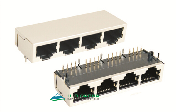
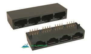
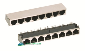

| Part Number: | ULO | - | PJ517 | - | S | 8 | 0 | B | P |
|---|---|---|---|---|---|---|---|---|---|
| Explanation: |
Brand ULO - ULO |
Model PJ517 - 4 ports in one row; shielded |
Connector Type S - Socket |
Contacts per Port 4 - 8P4C |
Plating 0 - Gold flash |
Colour B - Black |
Material P - PBT |
These right-angle, through-hole modular PCB sockets provide eight housing positions per port. P denotes housing positions and C denotes populated contacts: 8P4C has four contacts, 8P6C has six and 8P8C has eight. Choose the port arrangement, shielding and contact population together.
| Model | Ports | Arrangement | Construction | Contact options per port |
|---|---|---|---|---|
| ULO-PJ517 | 4 | Single row | Metal shield | 8P4C / 8P6C / 8P8C |
| ULO-PJ517A | 4 | Single row | Without metal shield | 8P4C / 8P6C / 8P8C |
| ULO-PJ518 | 8 | Single row | Metal shield | 8P4C / 8P6C / 8P8C |
| ULO-PJ519 | 8 | Two rows of four | Metal shield | 8P4C / 8P6C / 8P8C |
| Characteristic | Value | Applicability |
|---|---|---|
| Insulation resistance | ≥1000MΩ | All models |
| Dielectric withstand test | 500VAC for 1 minute | All models |
| Mating life | ≥600 cycles | All models |
| Insulator | PBT or nylon; material group I | All models |
| Flammability options | UL94V-0 or UL94V-2 | Exact grade-to-polymer assignment unspecified |
| Contacts | Copper alloy | All models |
| Shield | Copper alloy | PJ517, PJ518 and PJ519 |
The 500VAC value specifies a dielectric test. Working voltage, current rating, operating temperature and transmission performance are unspecified.
| Field | Code | Selection |
|---|---|---|
| Connector type | S | Socket |
| Contacts per port | 4 / 6 / 8 | 8P4C / 8P6C / 8P8C |
| Contact finish | 0 | Gold flash |
| Contact finish | 3 | Selective 3µin gold |
| Additional gold thickness options | Exact suffix unspecified | 6µin / 15µin / 30µin |
| Insulator colour | B | Black |
| Insulator material | P / N | PBT / nylon |
The five fields follow the model code in this order: connector type, contact population, contact finish, colour and material. The drawings show 8P8C bottom views and the full contact-hole patterns.
Dimensions below are in millimetres. Use the complete drawing for the selected model when laying out locating holes, shield tails and contact rows.
| Reference | PJ517 | PJ517A | PJ518 | PJ519 |
|---|---|---|---|---|
| Body width | 59.06 | 58.50 | 114.94 | 59.19 |
| Body depth | 21.27 | 20.60 | 21.27 | 28.30 |
| Body height | 13.50 | 12.80 | 13.50 | 25.30 |
| Port pitch within a row | 13.97 | 13.97 | 13.97 | 13.97; three intervals total 41.91 |
| Full contact-hole pattern | 32 × Ø1.20 | 32 × Ø1.20 | 64 × Ø1.20 | 64 × Ø0.90 |
| Adjacent stagger reference | 1.27 | 1.27 | 1.27 | 1.27 |
| Contact spacing within a row | 2.54 | 2.54 | 2.54 | 2.54 |
| Contact-row spacing within each port pattern | 2.54 | 2.54 | 2.54 | 2.54 |
| Locating holes | 2 × Ø3.25 | 2 × Ø3.25 | 2 × Ø3.25 | Two holes shown; diameter unspecified |
| Locating-hole centres | 53.34 | 53.34 | 109.22 | 53.34 |
| Shield-tail holes | 5 × Ø1.60 | Not applicable | 5 × Ø1.60 | 5 × Ø1.60 |
| PCB layout tolerance | ±0.05 | ±0.05 | ±0.05 | ±0.05 |
PJ517 has a 58.81mm outer shield-tail span. The PCB drawing gives an 8.89mm contact-row offset from the locating-hole line, a 3.68mm lower shield-tail offset and a 1.35mm local reference. The side view identifies 10.89mm and 8.89mm references around the locating feature. Mating-contact pitch is 1.02mm.


PJ517A omits the outer metal shield and its PCB tails. It retains a 53.34mm locating-centre span and 13.97mm port pitch, with a smaller body. The side view shows 10.16mm and 9.15mm references; the PCB contact-row offset is 8.89mm. Mating-contact pitch is 1.02mm.
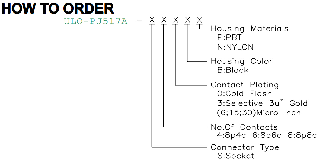

PJ518 places all eight ports in one row. Its outer shield-tail span is 114.69mm, with 109.22mm locating-hole centres. The PCB layout gives an 8.89mm contact-row offset and a 4.57mm lower shield-tail offset. The mating-contact detail identifies 1.02mm pitch and a 0.44mm contact reference; the side view includes a 10.89mm upper reference.


PJ519 uses two rows of four ports. The PCB pattern has four contact rows and separate shield-tail positions. Horizontal shield references are 58.92mm and 57.59mm. Vertical PCB references include 5.85mm, 4.57mm, 8.89mm, 11.43mm, 9.15mm and 15.50mm; the lowest shield-tail row is 1.35mm beyond the adjacent contact row. The side view gives the additional 15.47mm, 5.15mm, 4.75mm, 10.80mm and 12.93mm tail and housing references shown below.