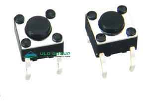
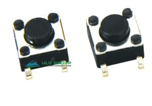
MDS429, MDS497 and MDS497A provide tactile SPST switching with model-specific body sizes, actuator heights and PCB patterns. Through-hole and surface-mount versions use different terminal geometry. Four-terminal circuits include two internally connected terminal pairs; they do not provide four independent switch poles.
Model
Nominal body options
PCB connection
Terminal arrangement
ULO-MDS429
12mm × 12mm
Through-hole
Four terminals on a 12.50mm × 5.00mm pattern; two additional locating holes
ULO-MDS497
6mm × 6mm; 3mm × 6mm
Through-hole
Four-terminal 6.5mm × 4.5mm pattern or two-terminal 6.5mm spacing
ULO-MDS497A
6mm × 6mm; 3mm × 6mm
SMT
Four-pad or two-pad patterns with 7.4mm pad-centre span
Electrical and environmental data
Characteristic
MDS429
MDS497 and MDS497A
Switch circuit
SPST momentary, normally open
SPST momentary, normally open
Contact rating
Unspecified
50mA at 12VDC
Contact resistance
≤100mΩ
≤100mΩ
Insulation resistance
≥1000MΩ
≥100MΩ
Withstand test
250VAC for 1 minute
Unspecified
Operating life
10000 cycles
10000 cycles
Operating temperature
-20°C to +70°C
-25°C to +70°C
Storage temperature
-45°C to +110°C
Unspecified
Static-load test entry
Unspecified
3kgf with switch placed vertically; test direction and duration not fully defined
The MDS429 withstand test is not a continuous working-voltage rating. The 3kgf static-load entry is not an operating-force specification; operating force is not separately stated.
MDS429 ordering choices keep actuator and housing colours independent.
MDS429 mounting and circuit
The body measures 12mm × 12mm. Four Ø1.30mm PCB holes lie on a 12.50mm × 5.00mm pattern; two Ø1.60mm locating holes use the illustrated 9.00mm separation. Recommended PCB layout tolerance is ±0.05mm. The terminal outline includes 13.9mm overall span, 0.3mm terminal thickness, 1.5mm terminal width, 3.5mm projecting section and 1.8mm end reference.
The drawing shows covered and uncovered actuator profiles, with H measured at its indicated reference. The actuator detail includes Ø7.1mm, 0.5mm maximum movement and a 3mm cover reference. In the schematic, T1/T2 form one internally connected pair and T3/T4 the other; pressing the actuator closes the connection between those pairs.
MDS429 12mm switch dimensions, cover profiles and terminal-pair circuit.
Ø3.5mm actuator; 0.7mm terminal width; 0.9mm upper side reference
Two-terminal narrow body
Two Ø1.0mm holes; 6.5mm centres
Ø3.5mm actuator; 1mm side terminal reference
Four-terminal long actuator
Four Ø1.0mm holes; 6.5mm × 4.5mm centres
Ø3.3mm actuator; 0.7mm terminal width; 1mm upper side reference
Outlines show 7.9mm overall lead span, 0.3mm terminal thickness, 3.6mm housing reference and 0.4mm maximum actuator movement. Lower lead projections are 3.5mm on the round-button outlines and 3.3mm on the long-actuator outline, with a 1.8mm end section. PCB layout tolerance is ±0.05mm. Four-terminal circuits connect 1/2 internally and 3/4 internally; the two-terminal circuit retains terminals 1 and 3.
MDS497 through-hole footprints and their separate circuit diagrams.
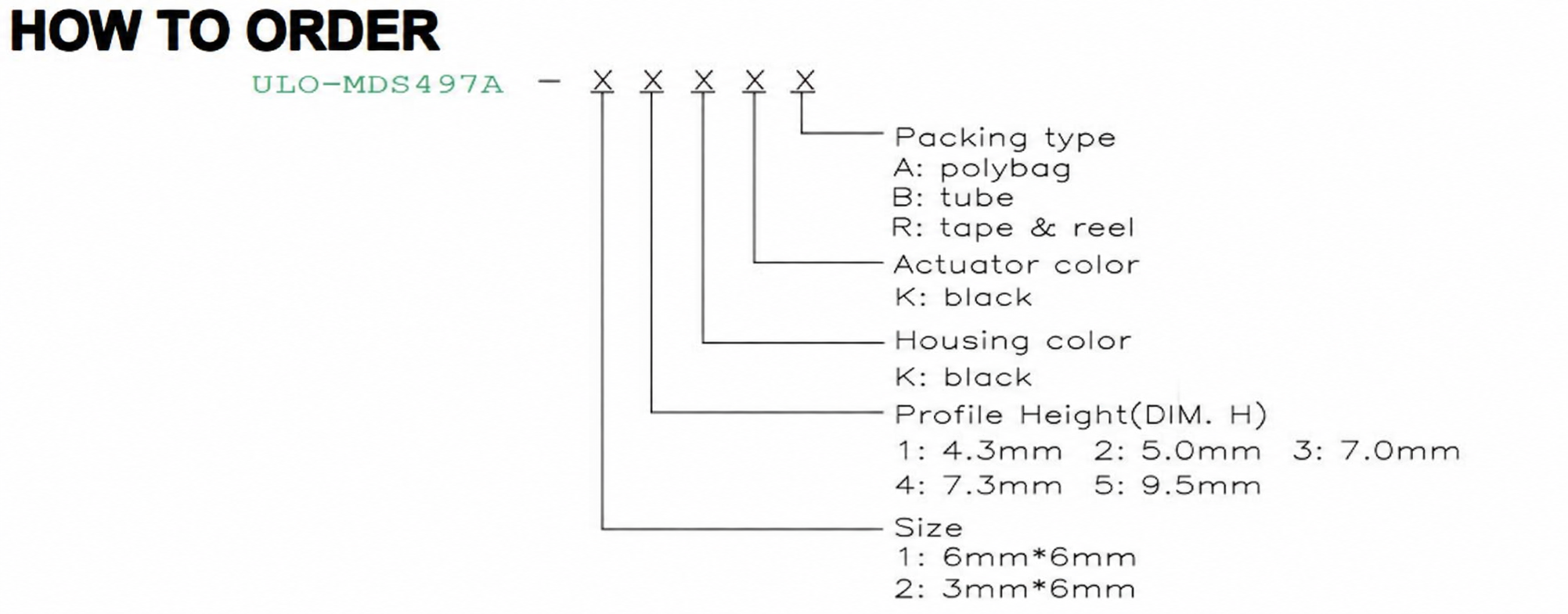
MDS497A ordering options
Field
Code or choice
Size
1: 6mm × 6mm; 2: 3mm × 6mm
Profile height H
1: 4.3mm; 2: 5.0mm; 3: 7.0mm; 4: 7.3mm; 5: 9.5mm
Housing colour
K: black
Actuator colour
K: black
Packaging
A: polybag; B: tube; R: tape and reel
MDS497A SMT switch ordering options.
MDS497A SMT patterns
Configuration
PCB footprint
Body and actuator references
Four-terminal body
7.4mm pad-centre span; 4.5mm between pad rows; 1.2mm pad-width reference; 9mm overall footprint span
3.0mm actuator reference; 1.5mm upper side reference; 0.70mm terminal width
Both drawings show a 3.5mm housing section and 0.5mm maximum actuator movement. Recommended PCB layout tolerance is ±0.05mm. The four-terminal SMT schematic connects 1/2 as one side and 3/4 as the other, with the numbers arranged differently from the through-hole drawing; the two-terminal SMT circuit uses terminals 1 and 2. Use the exact model's footprint and schematic when assigning PCB nets.
MDS497A surface-mount outlines and configuration-specific terminal numbering.
Soldering conditions for MDS497 and MDS497A
Process
Specified condition
Wave soldering
260°C maximum for 5 seconds, with 1.6mm PCB thickness
Manual soldering
30W soldering iron controlled at approximately 320°C for approximately 2 seconds
These conditions apply to MDS497 and MDS497A. A separate reflow profile and MDS429 soldering process are not specified.