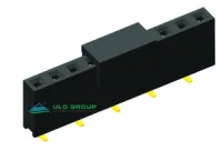
FH411 and FH412 variants cover vertical, right-angle, surface-mount, clip-board and extended-tail female headers. Select the exact model, row count, positions per row, body height, termination geometry and plating before laying out the PCB. A shared 2.54mm mating pitch does not make their footprints or installed heights interchangeable.
In the dimensional formulas below, N is the number of positions per row: total contacts for a single row, half the total for two rows and one third for three rows. A range such as 2×2–2×40 means two rows with 2–40 positions in each row. Height and tail options remain model-specific.
Common characteristic
Value
Mating pitch
2.54mm
Insulation resistance
≥1000MΩ
Dielectric withstand test
500VAC for 1 minute; FH411F–FH411T and FH412–FH412F specify RMS voltage
Insulation classification
Material group I; UL94V-0
Contact material
Copper alloy
Models
Current
Contact resistance
Operating temperature
Storage temperature
Insulator
FH411
Unspecified
≤20mΩ
0°C to +85°C
-20°C to +70°C
PA46
FH411A
3A
≤20mΩ
-20°C to +80°C
-20°C to +70°C
PA46
FH411B
3A
≤30mΩ
-20°C to +80°C
Unspecified
PA46
FH411C, FH411D, FH411E
Unspecified
≤50mΩ
0°C to +85°C
-20°C to +70°C
Glass-filled PBT
FH411F–FH411T; FH412–FH412F
3A
≤20mΩ
-45°C to +110°C
Unspecified
High-temperature material with 30% glass fibre; base polymer unspecified
Additional characteristic
Applicable models
Value or condition
Retention
FH411; FH411F–FH411T; FH412–FH412F
≥500gf
Resistance to soldering heat
FH411E only
260±5°C for 5±0.5s
The withstand test is separate from an operating-voltage rating. Soldering conditions and current ratings shown for one model do not extend to models with unspecified values. Full gold flash, selective gold flash and nickel plus gold flash are separate ordering choices; no coating thickness is assigned where unspecified.
FH411: one, two or three straight rows
Selection or reference
FH411
Contact arrangements
1×1–1×40; 2×2–2×40; 3×3–3×40
Ordering sequence
Contacts → S straight → plating → height
Plating codes
0: selective gold flash; F1: full gold flash; 2: nickel plus gold flash
FH411D ordering options.FH411D extended stack with different upper and lower pin sections.
FH411E: dual-row spacer and long tails
Selection or reference
FH411E
Ordering sequence
2×1–2×40 → B black → 8 full gold flash or 0 selective gold flash
Dimension type 1
A: 13.50mm; B tail extension: 6.50mm
Dimension type 2
A: 11.05mm; B tail extension: 2.50mm
Socket section and width
8.50mm socket section; 5.08mm body width
Length and contact span
(2.54N+0.5)mm and 2.54(N−1)mm
Tails and PCB
0.64×0.40mm tails; Ø1.02mm holes on 2.54mm row and position centres; layout tolerance ±0.05mm
Choose the A/B dimension pair together; the two pairs describe different spacer and tail arrangements.
FH411E ordering fields.FH411E spacer types and corresponding tail dimensions.
FH411F and FH411G: 6.8mm vertical bodies
Selection or reference
FH411F
FH411G
Contact range
1×1–1×40
2×1–2×40
Ordering after contact count
V vertical → 8 full gold flash or 0 selective gold flash
V vertical → 8 full gold flash or 0 selective gold flash
Body width / height
3.50mm / 6.80mm
5.80mm / 6.80mm
Body length / span
(2.54N+0.5)mm / 2.54(N−1)mm
(2.54N+0.5)mm / 2.54(N−1)mm
Contact-point depth reference
3–4mm
3–4mm
Tail section / projection
0.70×0.20mm / 3.30mm
0.70×0.20mm / 3.30mm
PCB
One row of Ø1.02mm holes at 2.54mm; ±0.05mm
Two rows of Ø1.02mm holes on 2.54mm grid; ±0.05mm
FH411F single-row ordering options.FH411F section, contact-point depth and PCB hole pattern.FH411G dual-row ordering options.FH411G wider body and two-row PCB hole pattern.
FH411H and FH411I: 7.1mm vertical bodies
Selection or reference
FH411H
FH411I
Contact range
1×1–1×40
2×1–2×40
Ordering after contact count
V vertical → 8 full gold flash or 0 selective gold flash
V vertical → 8 full gold flash or 0 selective gold flash
Body width / height
2.50mm / 7.10mm
5mm / 7.10mm
Body length / span
(2.54N+0.5)mm / 2.54(N−1)mm
(2.54N+0.5)mm / 2.54(N−1)mm
Tail section / projection
0.65×0.25mm / 3mm
0.64×0.25mm / 3mm
PCB
One row of Ø1.02mm holes at 2.54mm; ±0.05mm
Two rows of Ø1.02mm holes on 2.54mm grid; ±0.05mm
FH411H contact count, vertical mount and plating.FH411H body section and PCB hole layout.FH411I contact count, vertical mount and plating.FH411I body section and two-row PCB hole layout.
FH411J: single-row SMT with R1 or R2 tails
Selection or reference
FH411J
Ordering sequence
1×1–1×40 → B black → plating → bend → pickup → packing → posts
Finish and bend codes
8: full gold flash; 0: selective gold flash. Bend 1: R1; 2: R2
Handling options
Pickup S: with, X: without; packing T: tray, R: tape on reel, B: tube; posts S: with, X: without
Body and terminations
7.10mm body height; 2.50mm body width; 7.40mm seating reference; 4.50mm tail spread; tails 0.50×0.25mm
Length / contact span
(2.54N+0.5)mm / 2.54(N−1)mm
Pickup and posts
Pickup length 8mm, width 4mm, side extent 4mm; Ø0.80mm posts project 0.80mm, separated by 2.54(N−2)mm
1mm pad width; 2.54mm pitch; 7.40mm outer pad extent and 2.80mm inner gap; Ø1.19mm post holes, 1.27mm offset from adjacent end contact station; ±0.05mm
FH411K pickup, packaging and post selections.FH411K outline, underside and recommended PCB pattern.
FH411L and FH411M: 8.5mm scalloped bodies
Selection or reference
FH411L
FH411M
Contact range
1×1–1×40
2×1–2×40
Ordering after contact count
V vertical → 8 full gold flash or 0 selective gold flash
V vertical → 8 full gold flash or 0 selective gold flash
Height / tail projection
8.50mm / 3.50mm
8.50mm / 3.50mm
Body-width references
3.75mm overall; top-view 2.25mm and 0.75mm scallop references
Top-view 5.50mm and 0.75mm scallop references
Length / span / tail section
(2.54N+0.5)mm / 2.54(N−1)mm / 0.80×0.30mm
(2.54N+0.5)mm / 2.54(N−1)mm / 0.80×0.30mm
PCB
Single row, Ø1.02mm holes at 2.54mm; ±0.05mm
Dual rows, Ø1.02mm holes on 2.54mm grid; ±0.05mm
FH411L single-row ordering fields.FH411L body, tail and single-row hole dimensions.FH411M dual-row ordering fields.FH411M body-width references and two-row hole layout.
FH411N: dual-row clip-board termination
Selection or reference
FH411N
Ordering sequence
2×1–2×40 → B clip-board type → 8 full gold flash or 0 selective gold flash → dimension A
Dimension A codes
1: 1.70mm; 2: 1.00mm
Body
5mm high, 5.08mm wide; length (2.54N+0.5)mm
Contact and termination references
Span 2.54(N−1)mm; 0.70×0.25mm terminals; 1mm opposed-terminal gap
Dimension A describes the formed termination below the body. It is distinct from the fixed 5mm housing height.
FH411N two-row contact range and dimension A codes.FH411N dual-row body with opposed clip-board terminals.
FH411O: dual-row SMT in two body heights
Selection or reference
FH411O
Ordering sequence
2×2–2×40 → B black → plating → pickup → packing → posts → height A
Follow the FH411P R1 or R2 pin 1 position. The outline identifies optional post spacing separately from the centreline openings illustrated in the pad views.
FH411S contact-count and plating codes.FH411S compact body and straight-tail dimensions.FH411T contact-count and plating codes.FH411T two-row body and tail dimensions.
FH412: single-row and dual-row right-angle
Selection or reference
FH412
Ordering sequence
1×1–1×40 or 2×2–2×40 → R right-angle → F1 full gold flash or 0 selective gold flash
R1 and R2 alternate the tail side in opposite patterns; R3 places the tails on one side. Use the matching view and the illustrated insertion direction when selecting the mating-pin length.
FH412D three bend codes and two housing heights.FH412D formed tails, PCB and mating-pin insertion references.
Ø1mm holes at 2.54mm along row; 7.62mm between rows; ±0.05mm
1.10mm pad width; 2.54mm along-row pitch; 7.20mm inner gap and 11.80mm outer extent; ±0.05mm
FH412E full gold-flash socket ordering.FH412E mating face, body and through-hole PCB pattern.FH412F full gold-flash socket ordering.FH412F seated height, terminal spread and SMT pad pattern.